
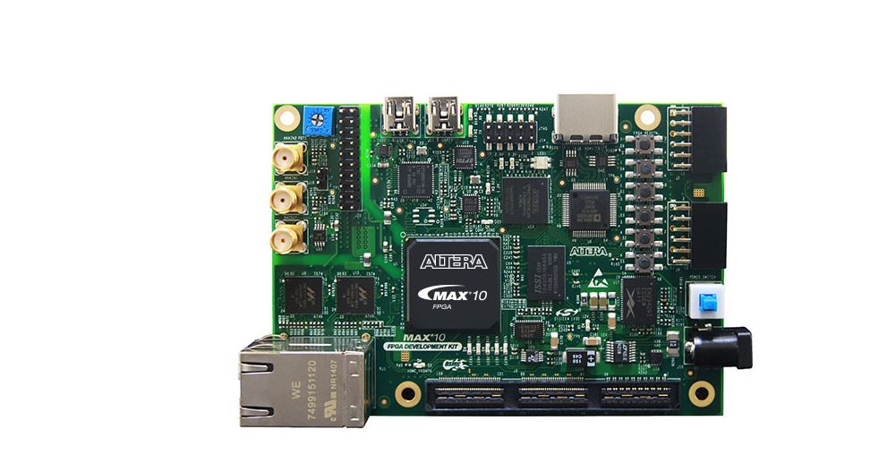
Terasic MAX 10 FPGA Development Kit
RoHS- and CE-compliant MAX 10 FPGA development board
Featured devices
MAX 10 FPGA (10M50D, dual supply, F484 package)
Enpirion® EN2342QI 4A PowerSoC voltage-mode synchronous step-down converter with integrated inductor
Enpirion EN6337QA 3A high-efficiency PowerSoC DC-DC step-down converters with integrated inductor
Enpirion EP5358xUI 600 mA PowerSoC DC-DC step-down converters with integrated inductor
MAX II CPLD – EPM1270M256C4N (On-board USB-Blaster II)
Programming and Configuration
Embedded USB-Blaster II (JTAG)
Optional JTAG direct via 10-pin header
Memory devices
64Mx16 1 Gb DDR3 SDRAM with soft memory controller
128Mx8 1 Gb DDR3 SDRAM with soft memory controller
512Mb quad serial peripheral interface (quad SPI) flash memory
Communication ports
Two Gigabit Ethernet (GbE) RJ-45 ports
One mini-USB2.0 UART
One HDMI video output
One universal HSMC connector (see HSMC expansion cards )
Two 12-pin Digilent Pmod™ Compatible connectors (see Pmod™ Compatible expansion cards )
Analog
Two MAX 10 FPGA ADC SMA inputs
2x10 ADC header
Potentiometer input to ADC
One external 16 bit digital-to-analog converter (DAC) device with SMA output
Clocking
25 MHz single-ended, external oscillator clock source
Silicon labs clock generator with programmable frequency GUI
Switches, push buttons, jumpers, and status LEDs
Mini-USB cable for on-board USB-Blaster II
2A power supply and cord
Free Quartus® Prime Lite design software (download software and license from the website)
Complete documentation
User manual, bill of materials, schematic, and board files
The Altera® MAX® 10 FPGA Development Kit provides a full featured design platform built around a 50 K logic elements (LEs) MAX 10 FPGA, optimized for system level integration with on-die analog-to-digital converter (ADC), dual-configuration flash, and DDR3 memory interface support. The board features on-board USB-BlasterTM II, high-speed mezannine card (HSMC), and Pmod™ Compatible expansion cards, high-definition multimedia interface (HDMI) output, and dual Ethernet for industrial Ethernet applications. The MAX 10 FPGA Development Kit provides the perfect system-level prototyping solution for industrial, automotive, consumer, and many other market applications.
With this development board, you can:
- Develop designs for the 10M50D, F484 package FPGA
- Measure the performance of the MAX 10 FPGA analog-to-digital block conversion
- Interface MAX 10 FPGAs to DDR3 memory at 300 MHz performance
- Run embedded Linux using the Nios® II processor
- Interface to daughtercards and peripherals using HSMC and Digilent Pmod™ Compatible connectors
- Measure FPGA power (VCC_CORE and VCC_IO ) using the power monitor graphical user interface (GUI)
- Reuse the kit’s PCB board and schematic as a model for your design
Get exclusive volume discounts, bulk pricing updates, and new product alerts delivered directly to your inbox.
By subscribing, you agree to our Terms of Service and Privacy Policy.
Direct access to our certified experts