
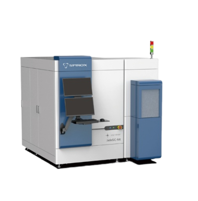
SPIROX SP3055A Non-Destructive Inspection System for SiC Crystal Killer-Defects (2” 4” 6” 8”, 300 μm - 550 μm)
SiC Substrate/EPI Wafer Size: 2” 4” 6” 8”
Wafer Thickness: 300 μm - 550 μm
Chuck: XY Stage Repeatability : 0.1 μm
Inspection Items: Whole Wafer Defect Scan (MicroPipe, BPD, TED, TSD, SF, etc.)
Whole Wafer Defect Scan
Estimated Inspection Time: 1 hr @4”wafer; 2 hrs @6”wafer; 4 hrs @8”wafer
Lateral Resolution: 1 μm
Analysis: MicroPipe Density (MPD); BPD/TED/TSD Density; Stacking Fault Area Percentage; Wafer Yield; Tri-angle and Carrot**
MicroArea 3D Scan (optional)
Field of View: 400 μm x 400 μm
Scanning Zoom: Yes ( 1x - 10x )
Scan Resolution: Up to 1024 x 1024
Lateral resolution: 0.4μm
Axial Resolution: 0.25μm
Min. Increment of Z stage: 0.02μm
Wide Field Module Camera: Color Camera (FOV 400 μm x 400 μm)
Get exclusive volume discounts, bulk pricing updates, and new product alerts delivered directly to your inbox.
By subscribing, you agree to our Terms of Service and Privacy Policy.
Direct access to our certified experts