
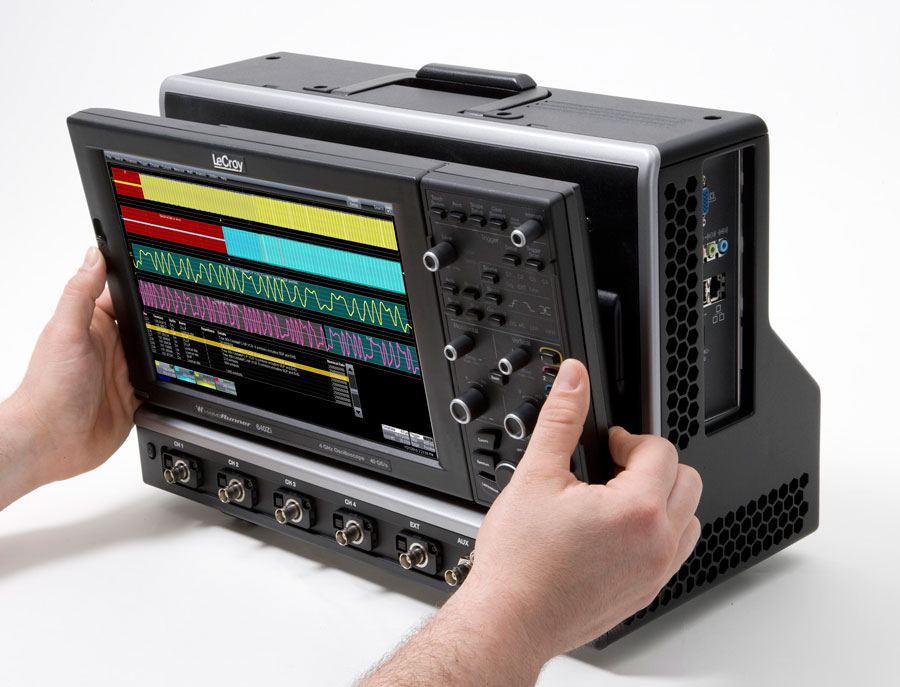
Lecroy WaveRunner 640Zi Oscilloscope (4Ghz, 20Gsa/s, 4 Ch)
ManufacturerLECROY(View more products from this manufacturer)
Model640Zi
Contact
Secure Checkout
Quality Engagement
Easy change and return
Delivery Available
Vertical System | |
| Nominal Analog Bandwidth @ Ω 50 10 mV-1 V/div | 4 GHz (≥ 5 mV/div) |
| Rise Time (10–90%) | 100 ps (typical) |
| Rise Time (20–80%) | 75 ps (typical) |
| Input Channels | 4 |
| Bandwidth Limiters | 20MHz, 200MHz, 1GHz |
| Input Impedance | 50 Ω±2% or 1 MΩ||17pF, 10 MΩ || 9.5 pF with supplied Probe |
| Maximum Input Voltage | 50 Ω: 5V RMS ± 10V peak 1 MΩ: 400 V max. (DC + peak AC < 10 kHz) |
| Channel-Channel Isolation | > 100:1 up to 2.5GHz > 50:1 from 2.5GHz to rated BW |
| Vertical Resolution | 8 bits; up to 11 bits with enhanced resolution (ERES) |
| Sensitivity | 50 Ω:1 mV/div - 1 V/div, fully variable 1 MΩ: 1 mV/div - 10 V/div, fully variable |
| DC Vertical Gain Accuracy (Gain Component of DC Accuracy) | ±1% F.S. (typical), offset at 0V; ±1.5% F.S. (test limit), offset at 0V |
| Offset Range | 50 Ω: BWL≤1 GHz ±1.6 V @ 2 mV - 4.95 mV ±4 V @ 5mV - 9.9 mV ±8 V @ 10mV - 19.8 mV ±10 V @ 20mV - 1V BWL>1GHz ±1.4V @ 5 mV-122mV/div ±10V @ 124 mV-1V/div 1 MΩ: ±1.6 V @ 2 mV - 4.95 mV ±4 V @ 5mV - 9.9 mV ±8 V @ 10mV - 19.8 mV ±16 V @ 20mV - 140 mV ±80 V @ 142mV - 1.4 V ±160 V @ 1.42mV - 10V |
| DC Vertical Offset Accuracy | ±(1.5% of offset setting +1% of full scale + 1 mV) (test limit) |
Horizontal System | |
| Clock Accuracy | ≤1.5 ppm +(aging of 0.5 ppm/yr from last calibration) |
| Trigger and Interpolator Jitter | ≤ 2 psrms (typical) <0.1 ps="" sub="">rms (typical, software assisted) |
| External Clock | DC to 100 MHz; (50 Ω/1 MΩ), EXT BNC input, Minimum rise time and amplitude requirements apply at low frequencies. |
Acquisition System | |
| Single-Shot Sample Rate/Ch | 20 GS/s on 4 Ch 40 GS/s on 2 Ch |
| Memory Options (4 Ch / 2 Ch / 1Ch) | S-32 Option: 32M / 64M / 64M (15,000) M-64 Option: 64M / 128M / 128M (15,000) |
| Standard Memory (4 Ch / 2 Ch / 1Ch) (Number of Segments) | 16 M / 32 M / 32M (4,500) |
Acquisition Processing | |
| Enhanced Resolution (ERES) | From 8.5 to 11 bits vertical resolution |
Triggering System | |
| Trigger Sensitivity with Edge Trigger ProBus Inputs | 2 div @ < 4 GHz 1.5 div @< 2 GHz 1 div @ < 200 MHz 0.9 div @<10 mhz="" br=""> |
| External Trigger Sensitivity, (Edge Trigger) | 2 div @ 1 GHz 1.5 div @ < 500 MHz 1 div @ <200 mhz="" br=""> |
| Max. Trigger Frequency, SMART Trigger | 2.0 GHz @ ≥ 10 mV/div (minimum triggerable width 200 ps) |
High Speed Serial Protocol Triggering | |
| Data Rates | 320 Mb/s - 3 Gb/s |
| Pattern Length | 80 bits, NRZ or 8b10b |
| Clock Recovery Jitter | 1 ps rms + 0.3% Unit Interval rms for PRBS data patterns with 50% transition density |
| Hardware Clock Recovery Loop BW | PLL Loop BW = Fbaud/5500, 100 Mb/s to 2.488 Gb/s (typical) |
LeCroy WaveStream™ Fast Viewing Mode | |
| Max Sampling Rate | 20 GS/s (40 GS/s when interleaved) |
Auxiliary Input | |
| Max. Input Voltage | 50 Ω: 5 Vrms; 1 MΩ: 250 Vmax (DC + Peak AC ≤ 10 kHz) |
Vertical System |
|
| Nominal Analog Bandwidth @ Ω 50 10 mV-1 V/div | 4 GHz (≥ 5 mV/div) |
| Rise Time (10–90%) | 100 ps (typical) |
| Rise Time (20–80%) | 75 ps (typical) |
| Input Channels | 4 |
| Bandwidth Limiters | 20MHz, 200MHz, 1GHz |
| Input Impedance | 50 Ω±2% or 1 MΩ||17pF, 10 MΩ || 9.5 pF with supplied Probe |
| Maximum Input Voltage | 50 Ω: 5V RMS ± 10V peak 1 MΩ: 400 V max. (DC + peak AC < 10 kHz) |
| Channel-Channel Isolation | > 100:1 up to 2.5GHz > 50:1 from 2.5GHz to rated BW |
| Vertical Resolution | 8 bits; up to 11 bits with enhanced resolution (ERES) |
| Sensitivity | 50 Ω:1 mV/div - 1 V/div, fully variable 1 MΩ: 1 mV/div - 10 V/div, fully variable |
| DC Vertical Gain Accuracy (Gain Component of DC Accuracy) | ±1% F.S. (typical), offset at 0V; ±1.5% F.S. (test limit), offset at 0V |
| Offset Range | 50 Ω: BWL≤1 GHz ±1.6 V @ 2 mV - 4.95 mV ±4 V @ 5mV - 9.9 mV ±8 V @ 10mV - 19.8 mV ±10 V @ 20mV - 1V BWL>1GHz ±1.4V @ 5 mV-122mV/div ±10V @ 124 mV-1V/div 1 MΩ: ±1.6 V @ 2 mV - 4.95 mV ±4 V @ 5mV - 9.9 mV ±8 V @ 10mV - 19.8 mV ±16 V @ 20mV - 140 mV ±80 V @ 142mV - 1.4 V ±160 V @ 1.42mV - 10V |
| DC Vertical Offset Accuracy | ±(1.5% of offset setting +1% of full scale + 1 mV) (test limit) |
Horizontal System |
|
| Clock Accuracy | ≤1.5 ppm +(aging of 0.5 ppm/yr from last calibration) |
| Trigger and Interpolator Jitter | ≤ 2 psrms (typical) <0.1 ps="" sub="">rms (typical, software assisted) |
| External Clock | DC to 100 MHz; (50 Ω/1 MΩ), EXT BNC input, Minimum rise time and amplitude requirements apply at low frequencies. |
Acquisition System |
|
| Single-Shot Sample Rate/Ch | 20 GS/s on 4 Ch 40 GS/s on 2 Ch |
| Memory Options (4 Ch / 2 Ch / 1Ch) | S-32 Option: 32M / 64M / 64M (15,000) M-64 Option: 64M / 128M / 128M (15,000) |
| Standard Memory (4 Ch / 2 Ch / 1Ch) (Number of Segments) | 16 M / 32 M / 32M (4,500) |
Acquisition Processing |
|
| Enhanced Resolution (ERES) | From 8.5 to 11 bits vertical resolution |
Triggering System |
|
| Trigger Sensitivity with Edge Trigger ProBus Inputs | 2 div @ < 4 GHz 1.5 div @< 2 GHz 1 div @ < 200 MHz 0.9 div @<10 mhz="" br=""> (DC, AC, and LFRej coupling, ≥ 10 mV/div, 50 Ω) |
| External Trigger Sensitivity, (Edge Trigger) | 2 div @ 1 GHz 1.5 div @ < 500 MHz 1 div @ <200 mhz="" br=""> 0.9 div @<10 mhz="" br=""> (DC, AC, and LFRej coupling) |
| Max. Trigger Frequency, SMART Trigger | 2.0 GHz @ ≥ 10 mV/div (minimum triggerable width 200 ps) |
High Speed Serial Protocol Triggering |
|
| Data Rates | 320 Mb/s - 3 Gb/s |
| Pattern Length | 80 bits, NRZ or 8b10b |
| Clock Recovery Jitter | 1 ps rms + 0.3% Unit Interval rms for PRBS data patterns with 50% transition density |
| Hardware Clock Recovery Loop BW | PLL Loop BW = Fbaud/5500, 100 Mb/s to 2.488 Gb/s (typical) |
LeCroy WaveStream™ Fast Viewing Mode |
|
| Max Sampling Rate | 20 GS/s (40 GS/s when interleaved) |
Auxiliary Input |
|
| Max. Input Voltage | 50 Ω: 5 Vrms; 1 MΩ: 250 Vmax (DC + Peak AC ≤ 10 kHz) |
Stay Updated with Offers
Get exclusive volume discounts, bulk pricing updates, and new product alerts delivered directly to your inbox.
By subscribing, you agree to our Terms of Service and Privacy Policy.
Quick Support
Direct access to our certified experts